


Blog
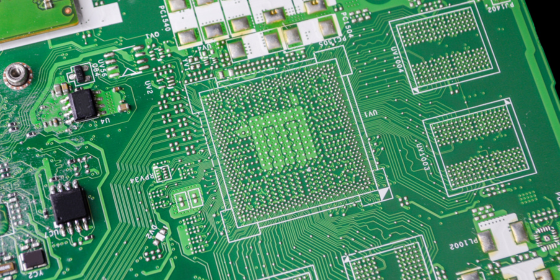
The PCB Fabrication Process
A step-by-step look at how PCBs are manufactured.
The PCB Fabrication Process
Read More
Editor's Picks
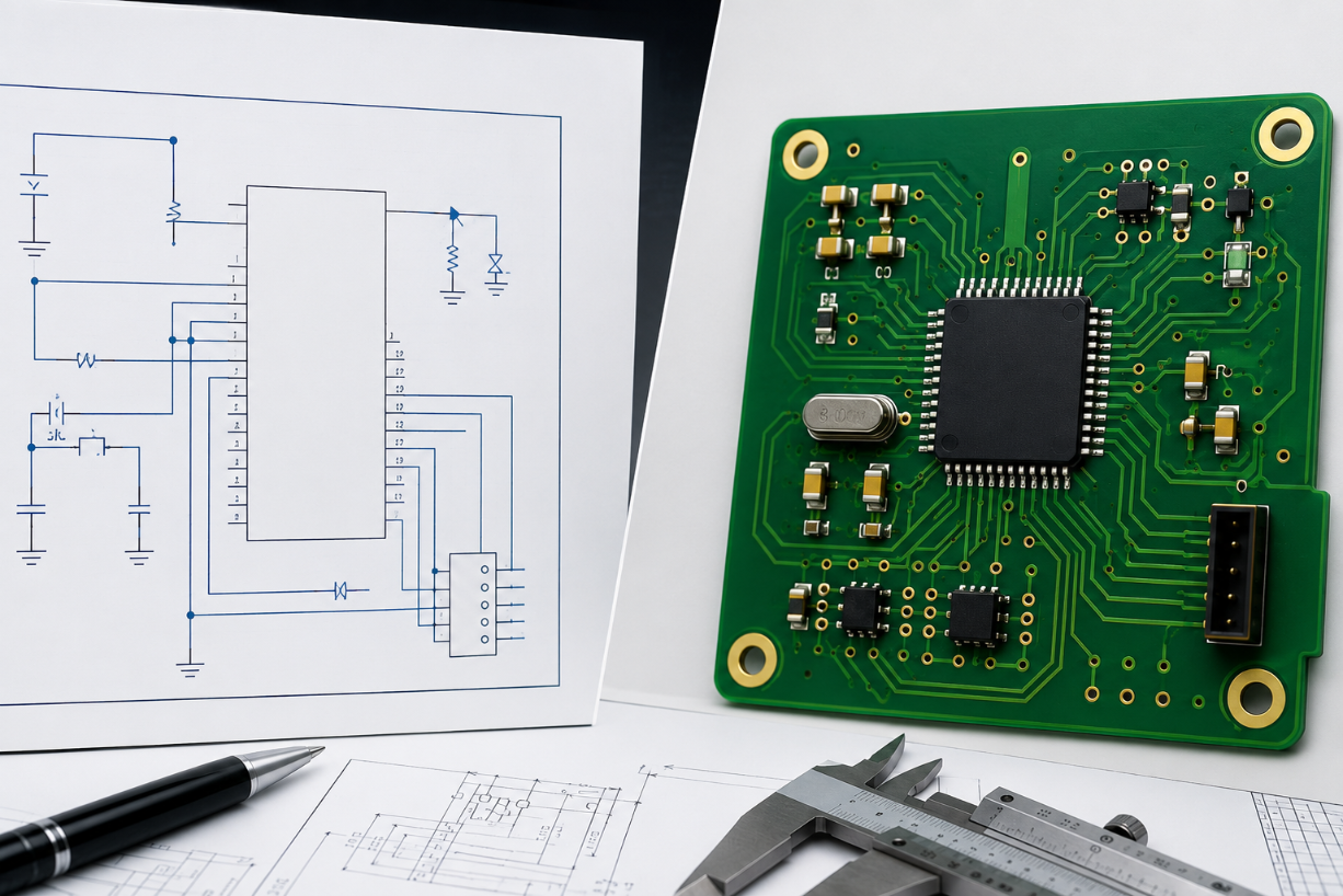
How to Keep Your Schematic and PCB Layout in Sync
Learn how to prevent schematic-to-PCB mismatches
How to Keep Your Schematic and PCB Layout in Sync
Read More

5 PCB Failures That Ground Drones, and How to Design Against Them
Learn the most common PCB failures in drone electronics, including vibration fatigue, thermal issues, RF interference, and thermal cycling, plus design strategies and IPC standards that improve UAV reliability.
5 PCB Failures That Ground Drones, and How to Design Against Them
Read More

RF Microwave PCB Design: Materials, Layout, and Manufacturing Best Practices
Learn RF microwave PCB design fundamentals including materials, impedance control, stackups, routing, testing, and manufacturing best practices.
RF Microwave PCB Design: Materials, Layout, and Manufacturing Best Practices
Read More
View All
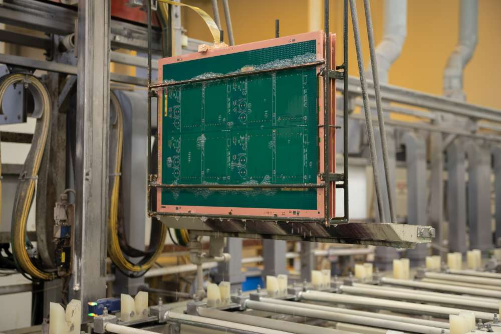
Meeting the Moment: Filling the Jobs in the Semiconductor Industry
The Semiconductor Industry Association, the foremost trade group in the space, projected that 67,000 of the new jobs the CHIPS Act will create are vulnerable to vacancy in 2030.
Meeting the Moment: Filling the Jobs in the Semiconductor Industry
Read More
d283.png)
Approaches to PCB Design for Signal Integrity and Manufacturability
fter formalizing a circuit’s functionality in a schematic diagram and deciding on the parts, devices, and technologies to employ, the next step is to create a functional PCB layout. This step aims to place all components on the PCB and establish all necessary connections, ensuring that the board dimensions are minimal and that application-specific goals, such as minimal losses or maximal signal integrity, are met.
Approaches to PCB Design for Signal Integrity and Manufacturability
Read More

Understanding High-Power PCB Requirements
Pinpointing what constitutes a high-power design can be challenging. However, high-power designs generally involve currents measuring multiple amperes or voltages extending into the kilovolt range.
Understanding High-Power PCB Requirements
Read More
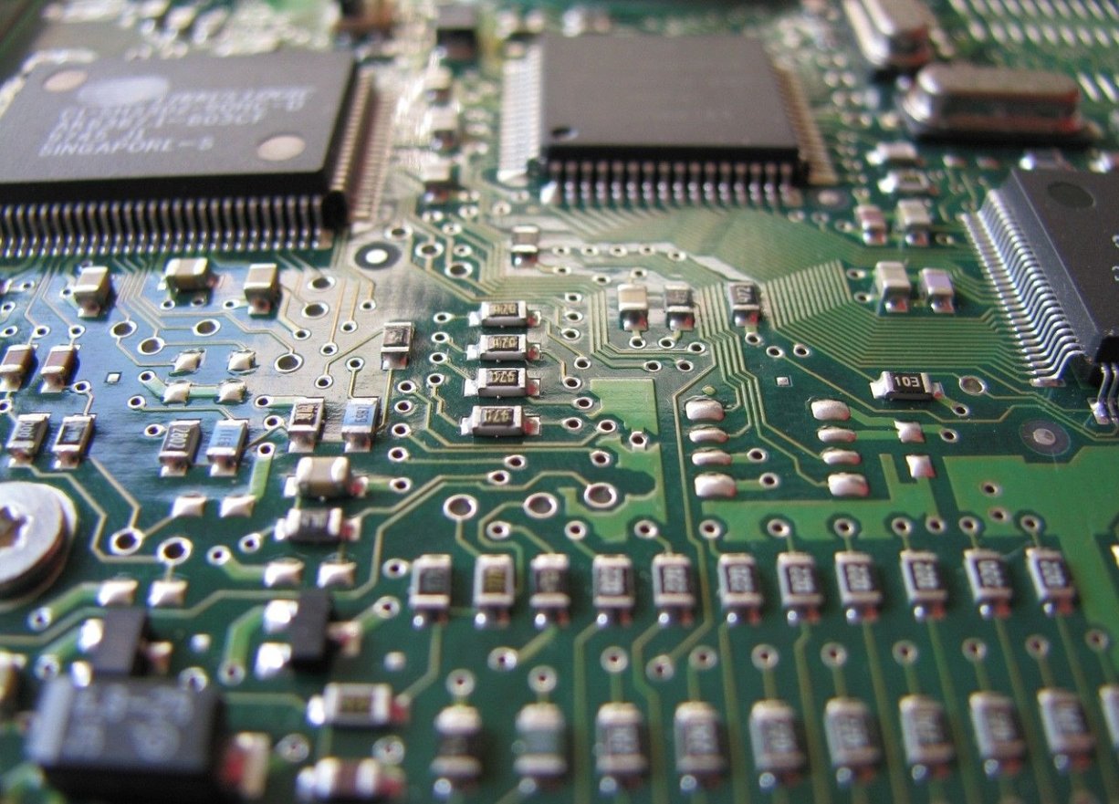
Through Hole vs Surface Mount: Performance and Cost Factors
Discover the differences between through hole vs surface mount components and find the best fit for your PCB projects at AdvancedPCB.
Through Hole vs Surface Mount: Performance and Cost Factors
Read More
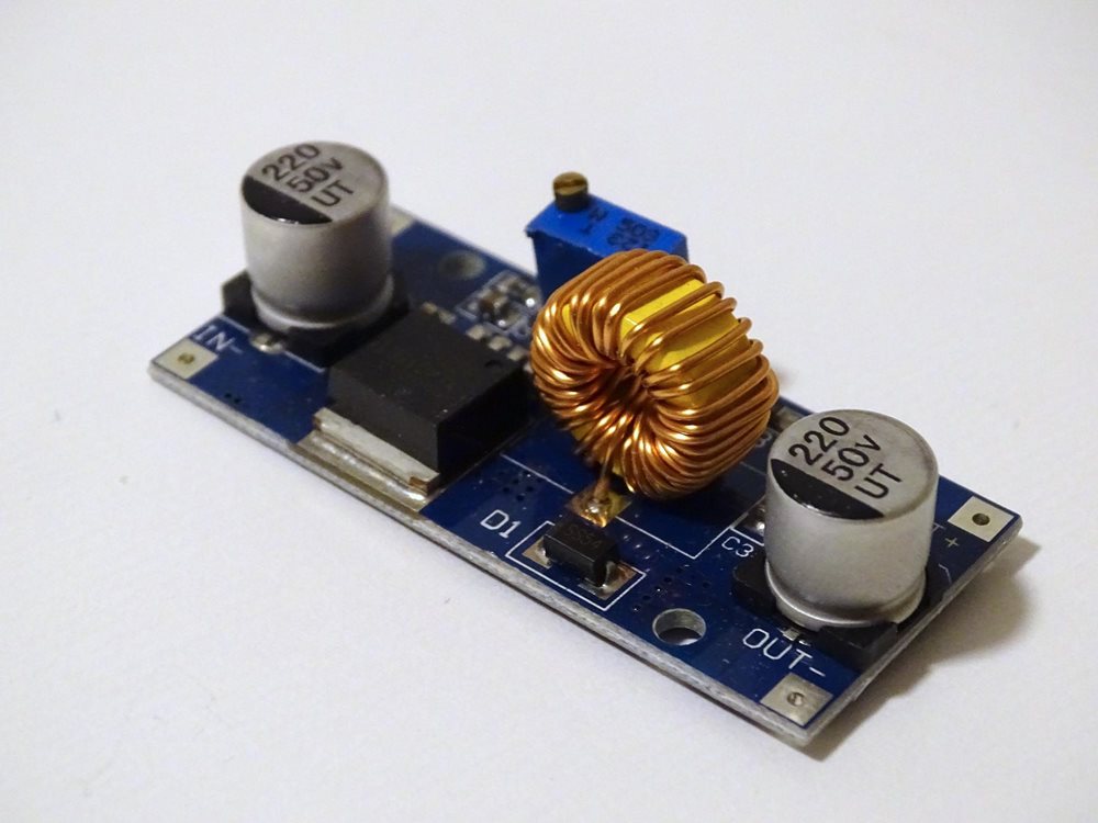
The Significance of Thermal Management in the PCB Design Process
Temperature influences electronic component behavior and characteristics in numerous ways. The effects are not limited to the components that get hot directly, but also those that are indirectly affected — for example, due to proximity or the PCB material’s thermal properties.
The Significance of Thermal Management in the PCB Design Process
Read More
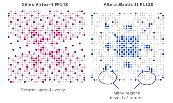
Managing Electromagnetic Interference in PCB Design
Ensuring electromagnetic (EMI) resistance and EMC compliance is paramount in designing PCBs, and adherence to standards is critical in multiple applications. EMI/EMC regulations govern the emission and susceptibility of electromagnetic radiation from electronic devices, ensuring that they operate harmoniously in their intended environments without causing interference with other devices.
Managing Electromagnetic Interference in PCB Design
Read More
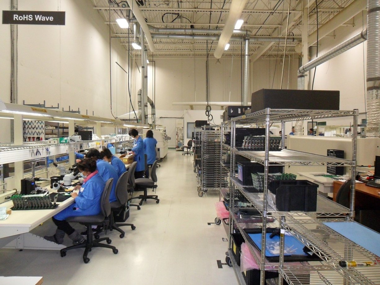
PCB Design Guidelines for DFM
Design for manufacturing (DFM) aims to create PCB designs that are functional, reliable, and testable while also meeting criteria that ensure the manufacturing house can reliably produce them at minimized costs. Designers can achieve DFM by understanding the basic steps involved in manufacturing PCBs, understanding key cost drivers, and following best-practice approaches across all phases of design.
PCB Design Guidelines for DFM
Read More
d283.jpg)
Overcoming Common Pitfalls in High-Frequency PCB Design
High frequency (HF) and radio frequency (RF) are fundamental in multiple domains, such as aerospace, defense, and medicine, and are often encountered in communication systems, radar devices, and imaging equipment. However, the high frequencies usually involve challenges that PCB designers would not typically face in non-HF designs, such as the need for impedance matching, the skin effect, crosstalk, EMI issues, and reflections.
Overcoming Common Pitfalls in High-Frequency PCB Design
Read More
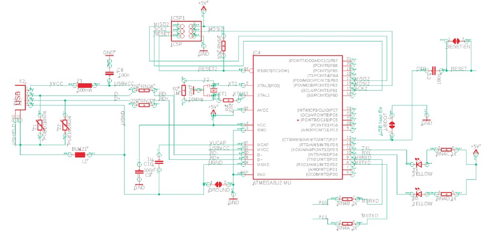
Demystifying the PCB Design and Manufacturing Process
Printed circuit boards (PCBs) form the vital backbone of practically all modern electronic devices, as they facilitate the production of intricate yet reliable designs in large quantities.
Demystifying the PCB Design and Manufacturing Process
Read More
Browse
All Categories